CROSS PROBING
Introduction
Cross-probing is a powerful technique for analysing and checking both your schematic and your PCB layout simultaneously. Essentially it allows you to take a schematic component and tag/zoom to the PCB footprint on the layout corresponding to that component. The Proteus design suite also enables you to look at a net on the schematic and highlight the same net on the PCB layout, thus allowing you to easily establish and check routing strategies and completeness.
Much of the cross-probing can be actioned directly from the application module you are working in (schematic vs layout) and/or you can work from within the Design Explorer. Where appropriate, we'll discuss both methods below.
Automatic Cross-Probing Mode (Design Explorer)
You can automate navigation to both schematic and layout modules by switching on the live cross-probing mode in the Design Explorer.

The live cross-probing toggle on the Design Explorer toolbar
When this is enabled, clicking on a component in the Design Explorer automatically tags the component part on the schematic and the footprint on the layout.
The difference between automatic mode and those described below is that there is no switch of tabs to the schematic or the layout in automatic mode. The most useful way to cross-probe in this way is therefore to detach the Design Explorer from the frame containing the schematic and layout by dragging the tab and dropping it. With the Design Explorer in a separate frame you can then click on a component and view the corresponding schematic and layout.
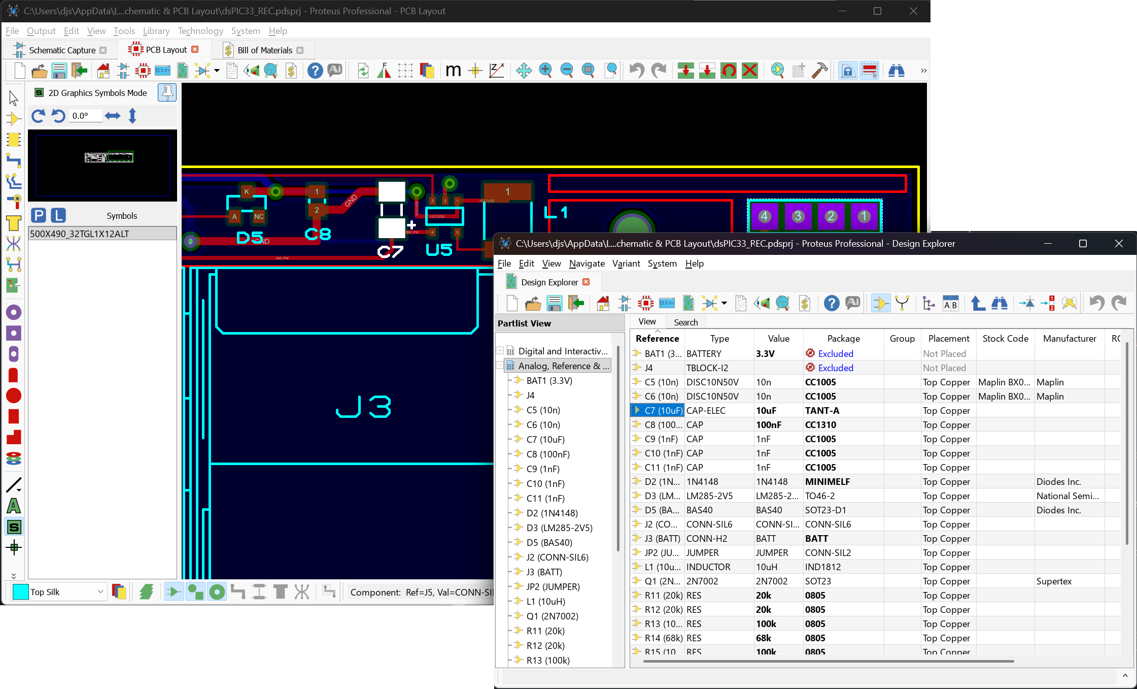
With live cross-probing on, selecting a part in the Design Explorer highlights it on both the schematic and the layout
Cross Probing to a Footprint
Direct from the Schematic
- Locate the component part that you want to cross-probe from.
- Right click and select Highlight Part in PCB Layout from the resulting context menu. The keyboard shortcut is ALT+P.
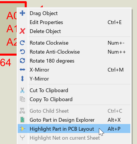
The Highlight Part in PCB Layout command on the schematic component context menu
Proteus will switch to (or launch) the Layout tab and navigate to the footprint corresponding to the component part on the schematic. Of course, if the footprint has not yet been placed on the layout not much will happen!
The same context menu carries Goto Part in Design Explorer (ALT+X), which takes you to the part in the Design Explorer rather than to the layout. This is the quickest way to reach the part when you want to inspect its properties or its packaging alongside the rest of the design.
Design Explorer
To cross probe to a footprint on the Layout :
- Make sure that both the schematic and the layout modules are open, have the design/layout file loaded and that they are synchronised (that is, that all changes made on the schematic have been netlisted through to the layout).
- Launch the Design Explorer.

- Make sure that you are in Partlist View, which is shown on the title bar of the Design Explorer.

- The right hand pane should be displaying a listing of component parts on the current schematic sheet.

- Right click on the schematic part of interest within this pane and you should get a context menu with a Show PCB Part option. Select this menu option and the layout module will both zoom to and highlight the footprint corresponding to the component you selected.

If the Show PCB Part option is greyed out then either the layout module is not open, does not have the layout corresponding to the open schematic loaded, or the schematic and PCB are out of sync. In the last case, turn on live netlisting in the layout module and repeat from step 2 above.
The Design Explorer stays open while you edit the schematic and updates to reflect the changes when you return to it, so you can leave it docked or detached into its own frame and work alongside it.
Cross Probing to a Net
Direct from the Schematic
Right clicking on a wire gives you three highlighting commands, each of which works on the whole net rather than on the single wire you clicked:
- Highlight Net on PCB Layout takes you to the layout and highlights every connection on the net there. This is the direct equivalent of Highlight Part in PCB Layout for connectivity.
- Highlight Net on current Sheet highlights the net where you are, which is useful for tracing a net through a densely wired sheet.
- Highlight Net on a Sheet opens a submenu listing the sheets in the design, so that you can follow a net across a multi-sheet design.
These commands need no Design Explorer and no view switching beyond the one the command performs, so they are the quickest route when you already have the net in front of you on the schematic.
Design Explorer
To cross probe to a net in the layout:
- Repeat steps 1 & 2 in Design Explorer above.
- Use the net icon at the top left of the Design Explorer to switch into Netlist View, which will be reflected on the title bar.

- The right hand pane will now be displaying a list of nets used in the schematic.

- Right click on the net of interest within this pane and you should get a context menu with a Show PCB Net option. Select this menu option and the PCB module will both zoom to and highlight the tracking on the net you selected.

Cross Probing from the Layout
Every route described above has a counterpart that starts on the PCB, so you can work in whichever module the question arises in.
- Right clicking on a footprint offers Show in Schematic (ALT+S), which switches to the schematic and highlights the component the footprint belongs to, and Show in Design Explorer (ALT+X).
- Right clicking on a track or a pad offers Highlight net on Schematic, the reciprocal of Highlight Net on PCB Layout, together with Highlight net on PCB Layout and Show net in Design Explorer.
- In the parts bin, right clicking on a footprint that has not yet been placed offers Show on Schematic, which is often the fastest way to work out where an unplaced part belongs.
The same prerequisites apply in this direction: the two modules must be open on the same project and in sync, or the cross-probe will either do nothing or land somewhere misleading.
See Also: